Frontier Introduction
According to a report by Nikkei Chinese Network, Nikkei XTECH and Nikkei ELECTRONICS conducted an overall analysis of the technical patents of Chinese and American chip companies using the patent analysis tool from the Japanese patent research company Patentfield.
From the overall data information, it can be seen that Chinese enterprises are catching up with American traditional enterprises in multiple fields such as GPU, transistor structures, and chip manufacturing technology. Moreover, they have made early technological layouts in advanced technology areas, engaging in long-term future competition with enterprises in the United States and South Korea. The determination of Chinese enterprises to seize the technological high ground in the chip industry has caused a sense of unknown fear among international companies.
Technical Patents
The Japanese institution compared Huawei, which is heavily sanctioned by the United States, with Intel and NVIDIA in the United States, and Samsung in South Korea.
In 2019, the number of patent applications for GPUs by Huawei began to show an upward trend. By 2023, Huawei's technical applications reached 3,091, representing nearly a tenfold increase compared to 2018, which was three times that of Intel and five times that of NVIDIA, but far less than Samsung Electronics.
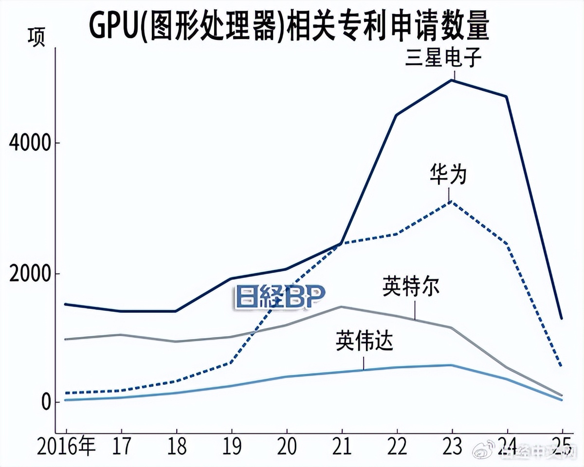
Samsung Electronics' large-scale patent applications are directly related to high-bandwidth memory. High-bandwidth memory works in collaboration with GPUs in the AI field. As a major player in the memory business, Samsung's large-scale technical applications also mark that Samsung is laying the groundwork for future AI industries.
In the most technically demanding areas of transistors and chip manufacturing, Huawei is also making slow progress.
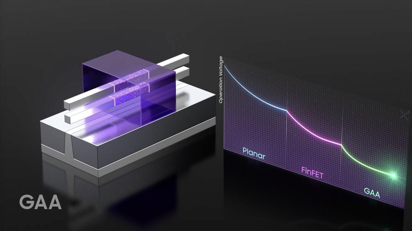
At present, the global chip industry believes that to advance chip technology into the next era of 2nm, the most direct technical solution is to use the GAA transistor structure.
The transistor structure of chips is divided into three stages. For processes above 14nm, planar transistor structures are used. For processes at 14nm and below, Fin FET transistor structures developed by Hui Zhengming are used. For processes at 2nm and below, GAA transistor structures are required.
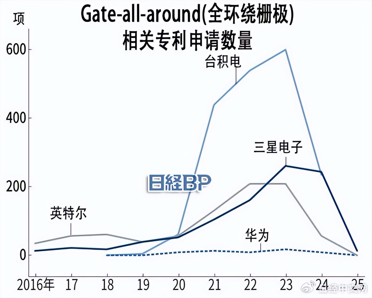
In the patent applications for the GAA structure, TSMC unquestionably became the leader among global companies. However, Huawei started its layout in 2018 and applied for about 20 relevant patents in 2023. Although the number is not large, Huawei continues to push forward. This gradual progress in the patent field indicates that Chinese enterprises are conducting research on 2nm chips in the future and are ready to engage in a prolonged battle with international giants.
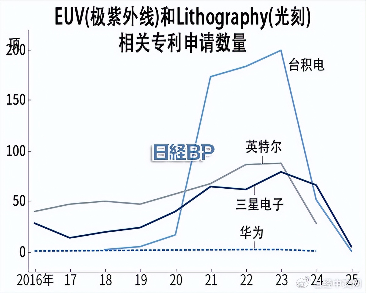
In terms of EUV and lithography technology patent applications, Huawei is also actively making arrangements. Due to U.S. sanctions and blockades, Chinese domestic companies cannot obtain advanced EUV lithography machines, which greatly restricts the progress of Chinese companies in developing independent advanced chips.
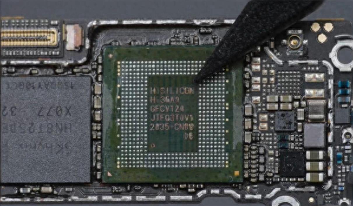
As one of the earliest companies blocked by the U.S. in chip development, Huawei does not involve chip manufacturing operations. Therefore, Huawei has the design capability but cannot manufacture and sell chips. This has forced Huawei to enter the chip manufacturing sector, starting to collaborate with domestic old-established wafer factories to solve the problem of advanced chip manufacturing.
Technical Pathways
Despite being blocked from EUV lithography machines, Chinese enterprises once purchased a batch of advanced immersion DUV lithography machines. These DUV lithography machines, combined with advanced etching machines and self-aligned multiple patterning technology (SAQP), can realize the manufacturing of 7nm chips.
According to Lin Benjian, former R&D vice president of TSMC, the requirement for overlay accuracy in multiple patterning technology is very high. Assuming an overlay CD deviation of 1.5%, if this deviation cannot be effectively resolved, it will ultimately lead to a sixth-order error of 8.4%, which is fatal for chip manufacturing.
Yang Guanglei, former head of R&D at TSMC and former director of SMIC, also stated in an interview that using immersion lithography machines that are slightly inferior to EUV to manufacture advanced chips is a feasible solution and a verified approach.
However, it is theoretically possible to continue manufacturing 5nm or even more advanced chips, but the yield rate is uncontrollable, and the resources invested are also uncontrollable. This is completely a technological no-man's land. Especially for Huawei, which has no foundation in chip manufacturing, this difficulty is even greater. It will take time to see results, and only through continuous experience accumulation can there be a chance of success.
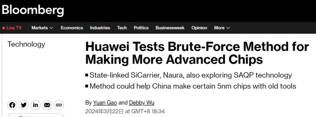
Bloomberg released a related report in 2024, pointing out that Huawei is collaborating with local chip companies to attempt to manufacture 5nm chips under limited equipment using traditional technical methods. This method is like forcing a solution, and currently, no enterprise on the international level has succeeded. TSMC, Samsung, and Intel have all shifted to EUV technology, while Chinese enterprises are the only ones currently using DUV lithography machines to challenge 5nm chips.
The future 2nm chip structure will transition from Fin FET to GAA. The gate inside the transistor will surround the nanosheet from all four sides, thus achieving better current control and minimizing quantum tunneling effects.
At present, Huawei has already been actively laying out the technical patents of transistor structures, starting from the basic structural level, gradually building a chip industry chain for Chinese enterprises. In the absence of solving the EUV lithography machine issue, using immersion lithography machines and self-aligned multiple patterning technology remains a compromise and a mature method.
The return of the Kirin chip marks that Chinese enterprises have successfully navigated the path of manufacturing advanced chips using multiple patterning technology. The next step is to continue reducing supply chain risks and achieve sustainable development in chip manufacturing. Under the condition of ensuring the safety and stability of the supply chain system, it is necessary to try to manufacture chips with new transistor structures using existing technical equipment.
References:
Nikkei BP Select: Looking at Huawei's Future Layout Through Patent Applications
Original: toutiao.com/article/7581702630921994802/
Disclaimer: This article represents the views of the author himself.