According to the WeChat official account "Fudan University," on the evening of the 8th, after half a year, following the release of the "Dawn (PoX)" picosecond flash device, Fudan University has made another milestone breakthrough in the engineering of two-dimensional electronic devices.
Recently, Fudan University announced that the "Changying (CY-01)" architecture developed by the team of Zhou Peng and Liu Chunsen integrates the "Dawn (PoX)" two-dimensional ultrafast flash device with mature silicon-based CMOS technology. It has successfully developed the world's first two-dimensional-silicon hybrid architecture chip.
The related research results were published in the journal Nature under the title "A full-featured 2D flash chip enabled by system integration" at 8:00 PM Beijing time on October 8th.

Two-dimensional-silicon hybrid architecture flash chip (with PCB board)
Fudan University stated that this breakthrough has solved the key challenges in the engineering of new two-dimensional information devices, providing an example for shortening the application cycle of the next generation of disruptive devices, and also offering strong support for promoting information technology into a new high-speed era.
In the era of big data and artificial intelligence, the performance of data access has been put to extreme requirements, while the speed and power consumption of traditional memory have become one of the "bottleneck" problems hindering the development of computing power. In April this year, the team of Zhou Peng and Liu Chunsen proposed the "Dawn" two-dimensional flash prototype device in the journal Nature, achieving ultra-high-speed non-volatile storage of 400 picoseconds, which is the fastest semiconductor charge storage technology so far, providing a fundamental principle to break the dilemma of computing power development.

"Dawn (PoX)" picosecond flash device
However, to truly move disruptive devices towards system-level applications, it is often a long marathon. Looking back at the development of silicon-based chips, since the birth of semiconductor transistors in 1947, after more than two decades of joint research by top forces such as Bell Labs, Fairchild, and Intel, the first CPU was finally born globally.
As a frontier field of integrated circuits, two-dimensional electronics has received much attention in recent years, but researchers are most concerned about the "LAB to FAB (from laboratory to factory)" problem, which is whether this technology can be truly applied in the future. How to accelerate industrialization and make two-dimensional electronic devices move towards functional chips?
"From the current technology, memory is the most likely type of two-dimensional electronic device to be industrialized first. Because it does not require higher material quality or process manufacturing, and the performance indicators it can achieve far exceed the current industrialized technologies, which may create some disruptive application scenarios." Zhou Peng, who has been working in the memory field for many years, said.
Currently, CMOS (Complementary Metal Oxide Semiconductor) technology is the mainstream process for integrated circuit manufacturing, and most integrated circuits in the market are manufactured using CMOS technology, with a relatively mature industry chain. The team believes that if they want to accelerate the incubation of new technologies, they need to fully integrate two-dimensional ultrafast flash devices into the traditional CMOS semiconductor production line, which can also bring new breakthroughs to CMOS technology.

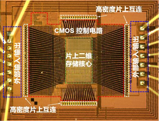
Schematic diagram of the two-dimensional-silicon hybrid architecture flash chip structure, including a two-dimensional module, CMOS control circuit, and micrometer-scale vias
To find this "correct path," the team experienced five years of exploration and trial and error, focusing on multiple points such as single devices and integration processes. Their first integration work was published in Nature Electronics in 2024, achieving a breakthrough in two-dimensional yield on the ideal native substrate, which provided a foundation for solving problems on real and complex CMOS substrates.
Chips today are mostly made of silicon materials. However, silicon materials and two-dimensional materials are completely different - the thickness of silicon wafers is often hundreds of micrometers, and even some thin silicon layers are at least tens of nanometers; while two-dimensional semiconductor materials are at the atomic level, equivalent to a thickness of less than 1 nanometer.
"As a new material system, two-dimensional semiconductors do not exist in any integrated circuit manufacturing factory around the world. Once a new material is introduced, it could have immeasurable effects on other electronic devices, potentially polluting the production line, which all chip manufacturers cannot accept," Zhou Peng introduced.
How to integrate two-dimensional materials with CMOS without damaging their performance is the core challenge the team needs to overcome. The surface of CMOS circuits has many components, like a miniature "city," with tall buildings and flat areas, uneven terrain; while two-dimensional semiconductor materials are only 1-3 atoms thick, like a "dragonfly wing," extremely thin and fragile. If two-dimensional materials are directly placed on CMOS circuits, the materials are easily broken, let alone achieving circuit performance.
"It's like looking at Shanghai from space, which seems flat, but the city actually has buildings of varying heights, such as 400 meters, 100 meters, or even dozens of meters. If we lay a film over the city, the film itself would be uneven," Zhou Peng gave a vivid analogy.
This is why researchers around the world can currently only process materials on extremely flat native substrates. One solution is to "flatten" the CMOS substrate to adapt to two-dimensional materials, but achieving atomic-level flatness is not realistic.
Optical microscope photo of the two-dimensional-silicon hybrid architecture flash chip
"We don't need to change CMOS, but instead need to adapt to it." The team decided to start with two-dimensional materials that have inherent flexibility, using a modular integration scheme to first fabricate two-dimensional memory circuits and mature CMOS circuits separately, then achieve complete chip integration through high-density monolithic interconnection technology (micrometer-scale vias).
It is this core process innovation that enables the tight bonding of two-dimensional materials and CMOS substrates at the atomic scale, ultimately achieving a chip yield of over 94%. The team further proposed a cross-platform system design methodology, including two-dimensional-CMOS circuit collaborative design and two-dimensional-CMOS cross-platform interface design, and named this system integration framework "Changying (CY-01) Architecture."
From basic research to engineering application, the team has crossed the most difficult step, and subsequent iterations will further accelerate. Their next plan is to establish an experimental base and collaborate with relevant institutions to build an independently led engineering project, and plan to integrate the project to the megalevel within 3-5 years, during which the generated intellectual property and IP can be licensed to partner companies.
In the era of artificial intelligence, the current AI system bottleneck is shifting from the front-end computing power to the back-end storage and data. Industry insiders believe that this achievement will enable faster transition from the laboratory to large-scale applications, integrating into personal computers, mobile devices, and other scenarios.
Representatives from the memory industry believe that the team's two-dimensional devices have an inherent advantage in access speed, which can break the balance of speed, power consumption, and integration of flash memory itself, and may bring greater market opportunities in the 3D application field. The next step is to expect collaborative efforts between industry, academia, and research to bring changes to the $60 billion market annually.
"This achievement is not just a successive technological improvement, but more of a disruptive progress in storage speed and efficiency," analyzed the representative of Fudan Investment. This technology has formed a "science-engineering-system" closed loop, meeting the demands of computing power and storage in the AI era, and by relying on the mature CMOS production line, it can shorten the R&D cycle and reduce the commercialization threshold.
"This is the 'source technology' of China's integrated circuit field, enabling China to take the initiative in the next generation of storage core technology fields." Looking ahead to the future of the two-dimensional-silicon hybrid architecture flash chip, the team of Zhou Peng and Liu Chunsen hopes that this technology will disrupt the traditional memory system, allowing general-purpose memory to replace multi-level hierarchical storage architectures, and provide faster and lower energy consumption data support for cutting-edge fields such as artificial intelligence and big data, making two-dimensional flash memory the standard storage solution in the AI era.
Original article: https://www.toutiao.com/article/7559237598552654362/
Statement: The article represents the views of the author. Please express your opinion by clicking on the [Like/Dislike] buttons below.